2006-01-06
Revision 1 - Kits sold in 2005
| Resistor | Nominal value | Delivered | Colour code |
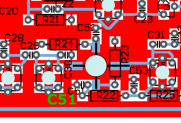
| R1, R22 | 27 kΩ | 27,4 kΩ | Red Violet Yellow Red Brown |
| R2, R23 | 10 kΩ | 10,0 kΩ | Brown Black Black Red Brown |
| R3, R14, R18 | 180 Ω | 182 Ω | Brown Grey Red Black Brown |
| R4, R7, R25, R29 | 22 Ω | 22,1 Ω | Red Red Brown Gold Brown |
| R5, R19 | 47 Ω | 47,5 Ω | Yellow Violet Green Gold Brown Red |
| R6, R17 | 150 Ω | 150 Ω | Brown Green Black Black Brown (Red) |
| R8 | 8,2 kΩ | 8,25 kΩ | Grey Red Green Brown Brown Red |
| R9 | 2,2 kΩ | 2,21 kΩ | Red Red Brown Brown Brown |
| R10 | 1,2 Ω | 1,21 Ω | Brown Red Brown Silver Brown Brown |
| R11 | 5,6 kΩ | 5,62 kΩ 5,49 kΩ |
Green Blue Red Brown Brown Red Green Yellow White Brown Brown Red |
| R12 | 15 kΩ | 15,0 kΩ | Brown Green Black Red Brown |
| R13, R26 | 1 kΩ | 1,00 kΩ | Brown Black Black Brown Brown |
| R15, R16, R24 | 39 Ω | 39,2 Ω | Orange White Red Gold Brown Red |
| R20 | 22 kΩ | 22,1 kΩ | Red Red Brown Red Brown Red |
| R21 | 3,3 kΩ | 3,32 kΩ | Orange Orange Red Brown Brown |
| R27 | 4,7 kΩ | 4,75 kΩ | Yellow Violet Green Brown Brown Red |
| R28 | 12 Ω | 12,1 Ω | Brown Red Brown Gold Brown Red |
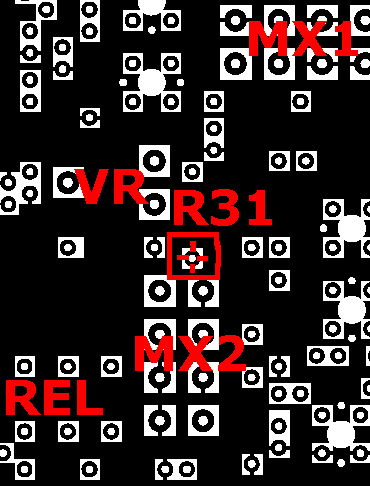
| R30, R31 | 82 Ω | 82,5 Ω | Grey Red Green Gold Brown |
| VR | 250 Ω | 220 Ω |
All resistors are 0,25 W/0,4 W and metal film type.
| Capasitor | Nominal value | Marking |
| C1, C7, C14, C24, C26, C32 | 120 pF | n12 |
| C2, C8, C28 | 27 pF | 27 |
| C3, C4, C30, C31 | 22 pF | 22 |
| C5, C6, C27, C29 | 1 pF | 1 |
| C9 | 270 pF | 271 |
| C10, C11, C25 | 33 pF | 33 |
| C12 | 3,3 pF | 3.3 |
| C13, C34, C35 | 39 pF | 39J 100V |
| C15 | 100 nF polyester, 2-modules | µ1K63, yellow |
| C16 | 1 µF, 100 V, electrolytic, axial | 1µ0/100V |
| C17, C18 | 22 µF, 25 V, electrolytic, axial | 22µ/25V |
| C19, C21 | 82 pF | 82 |
| C20 | 150 pF | n15 |
| C22 | 10 pF | 10 |
| C23 | 47 pF | 47 |
| C33 | 1 nF | 1n0, small yellow |
| C36, C37 | 12 pF | 12p, grey-green black top |
| C38-C58 | 10 nF | 10n, yellow green top/brown 103 |
All capacitors are 1 module, 2,54 mm, ceramic types unless otherwise stated.
| Component | Possible component | Delivered |
| D1, D2 | 5,6 V zener diode, 0,5 W | Blue |
| D3, D4 | 1N4004 or equivalent | 1N4006, black |
| D5, D6, D7 | 1N4148 or equivalent | 1N4148, red |
| IC1 | 78L08 | 78L08 |
| Q1, Q8 | BF988, BF981, BF900, BF960 | BF988, text facing down, D long terminal |
| Q2, Q7 | J310, U310 | J310 |
| Q3, Q4 | BD442, BD434, BD438, BD136, BD140 | BD442, Q3 metal facing west, Q4 metal facing east |
| Q5 | BC337 | BC337 |
| Q6 | BFW93, BFW92 | BFW93, text facing up, C long terminal |
| Q9 | BFR96 | BFR96, text facing up, C long terminal |
| Inductor | Type | Comments |
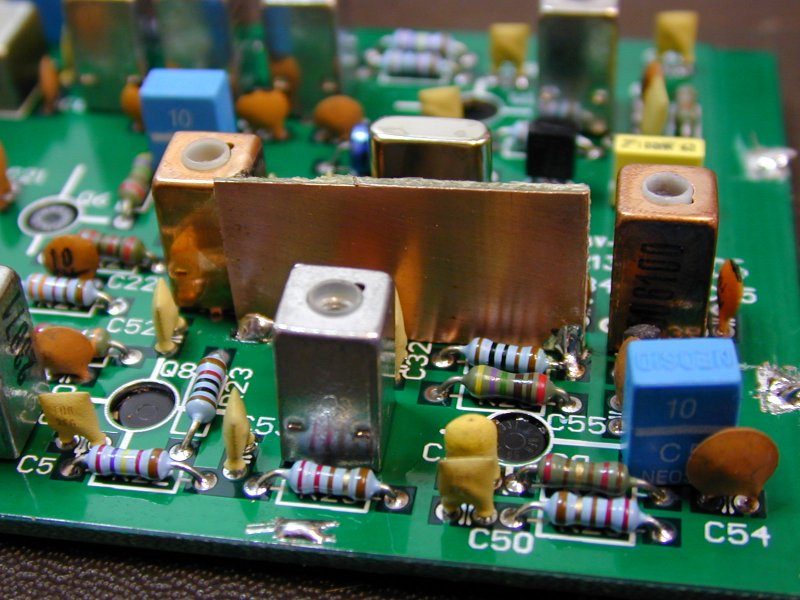
| DR1, DR2, DR6, DR8 | 10 µH | Neosid, blue plastic cap, 10 |
| DR2, DR6 | 18 µH | Neosid, blue plastic cap, 18 |
| DR3, DR4, DR5 | Ferrite bead | Run a piece of wire through the ferrite beads, big beads |
| DR7 | 15 µH RF-choke | Axial, Brown Green Black Silver |
| DR9 (Drain-choke) | Ferrite bead | To be mounted over Q1 drain terminal, small bead |
| L1, L2, L3, L4, L12, L13, L14, L15 | Neosid 00 5231 03 | Grey metal housing |
| L5, L16 | Neosid 00 5061 00 | Marked 5061 |
| L6, L7, L8 | Neosid 00 5048 00 | The top is marked with yellow and grey dots |
| L9, L10, L11 | Neosid 00 5049 00 | Marked 5049 |
L1-L16: In case the inductor has a fifth terminal, one that is not located in a corner, cut it away.
| MX1, MX2 | SBL-1, IE500, IE800, HPF-505 |
| Crystal | 42 MHz, third overtone, HC49/U |
| Metal sheet box | 148 x 74 x 30 mm3 |
| BNC-connectors | Four BNC-connectors. Remove the four terminals on each connectors. |
| Feed through capacitors | 1 nF, solderable into a 3,2 mm hole |
| Relay | Omron G5V-2 |
| 10 cm coax | Used in case of separate 28 MHz RX |
I have tested the same fix on another transverter and it had the opposite effect increasing the LO from -60 dBc to -50 dBc. Here are some successful LO screen ideas mounted on component side: Paul, GW8IZR, Tim, OZ4GA.
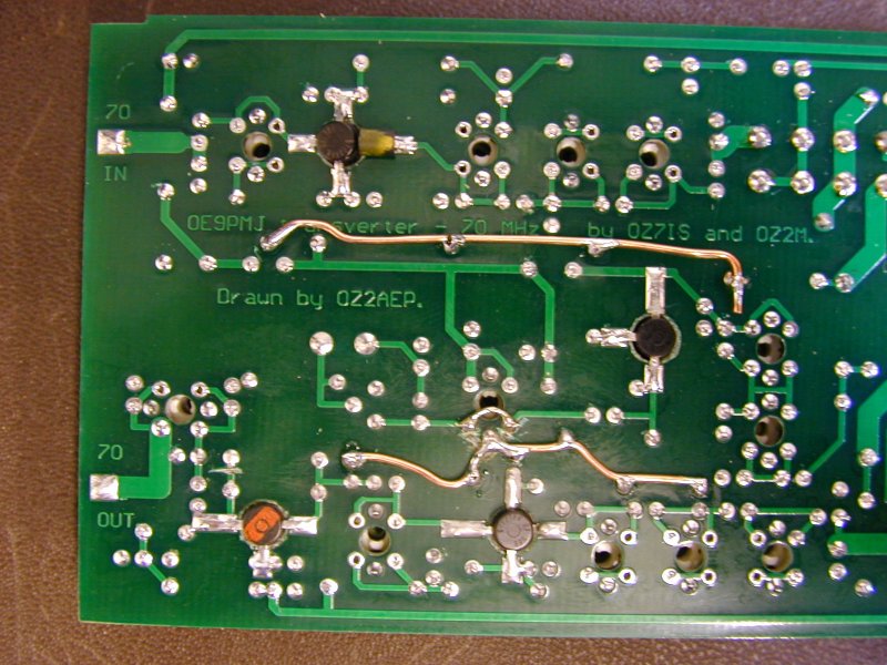
According to Paul, GW8IZR, a screen on the track side has even greater
effect than on the top side. See an example here.
Paul, GW8IZR, did some more research on the spurious and what seems to be
the solution is a screen on the trackside covering the oscillator circuit.
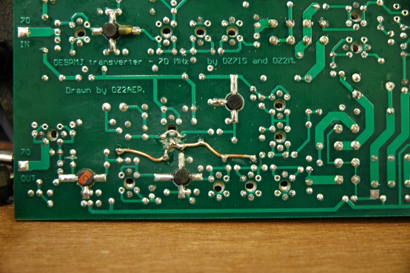
First he installed two ground rails,
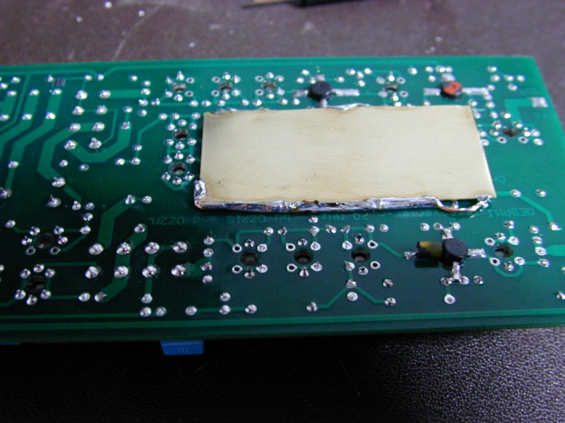
then added the screen plate and finally
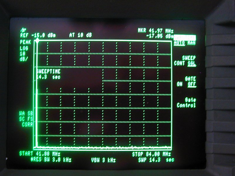
did this measurement showing no LO or
associated harmonics, i.e. all below -65 dBc and with out the topside
screen. However, the topscreen does not harm so if already installed leave
it.
Some transverters show a tendency to oscillate on the output. A way to cure this is by reducing the gain in Q8 by removing C52 results. Doing so reduces the TX gain about 6 dB. Paul, GW8IZR, has also tried to vary the supply voltage between 10 and 18 V and there is no sign of oscillation when the TX BPF has been sweeped.
Uffe, PA5DD, writes:
"By searching the Internet I found a reference to an old article in the German magazine
Funktelegramm. The article was written by Mike DL1GNM and should contain some changes to improve the stability of the original OE9PMJ transverter.
I E-mailed Mike, and the change was to place a 10 nF capacitor parallel to C33
(1 nF) - the emitter de-coupling of the final transistor Q9 (BFR96).
To my surprise, this changed the tuning of Q9 quite a bit - an indication, that the 10nF capacitor had quite an effect. At the same
time I have no more oscillations, even in the original configuration and "max smoke" tuning method. I did solder my extra 1 kΩ resistor at G1 of Q8 back in to decrease the gain a bit.
I reckon the 1 nF capacitor was chosen with regard to BFR96 being a microwave transistor, but it seems that it does not provide proper
decoupling at the working frequency due to the low impedance, at the emitter.
My conclusion is to add a 10 nF SMD on the backside of C33 if you experience instability in the transmitter."
Bo, OZ2M, www.rudius.net/oz2m