2023-01-17
![]()
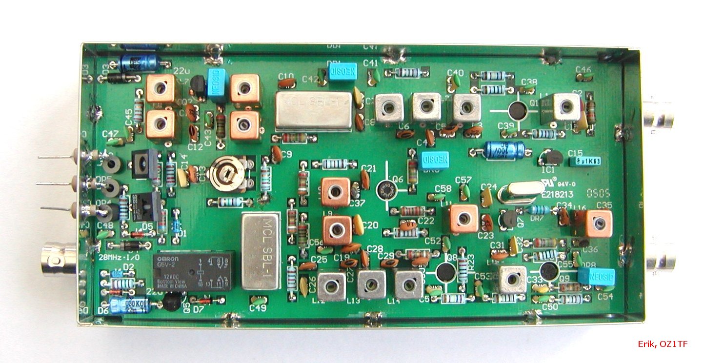
Transverter kit assembled by Bo, OZ1DJJ.
This page gives a brief description of a 70 MHz transverter that has been published in the Danish amateur radio magazine "OZ." This way hams outside Denmark may also benefit from the design.
Peter, PA2V, also published an article concerning the transverter in Elektron May 2005, the Dutch magazine issued by VERON.
Click here for power amplifier kit.
There are no more kits available.
Here is a list of the delivered components and changes etc.
A more thorough description of the circuit design can be found in the original 50 MHz transverter article found below.
When the 70 MHz band was introduced in Denmark during 2003 we all started up using whatever equipment available: 4 meter PMR radios, Yaesu FT-847, ready made transverters brought in from the UK, etc. As the FT-847 is the only available commercial radio, though not performing particularly good, - we started looking for a suitable transverter construction to publish in the Danish amateur radio magazine: "OZ", in order to boost the interest and activity on the four meter band in Denmark.
We adopted the late OE9PMJ, Peter Riml 50 MHz transverter construction, originally published in 1990. The design still seems rather modern and intuitive. No need to start from scratch. An important advantage: It is reproducible to most amateurs, as only conventional components are used in the construction. No microscopic SMD components, though the layout is relatively compact. Another advantage is that all inductors are available as ready-made components. All in all the construction is not hard to build to most amateurs, though some experience in RF constructions is an advantage!
The first unit was build without too many calculations by OZ7IS using plain common sense! A few experiments later it was working quite satisfactory. Unit two was copied from the first one and tested thoroughly by OZ2M in the following months while simulating and testing all circuits section by section on unit three. Several details were optimised and a few improvements relating to the original construction was made as well. Among other things we changed to a cheaper changeover relay. No need for expensive relays on 28 MHz! Consequently a new PCB layout was made by Erik, OZ1TF. It is still useable for 50 MHz though. Even with the cheap relay! All in all it is a proven and well-documented construction presented below.
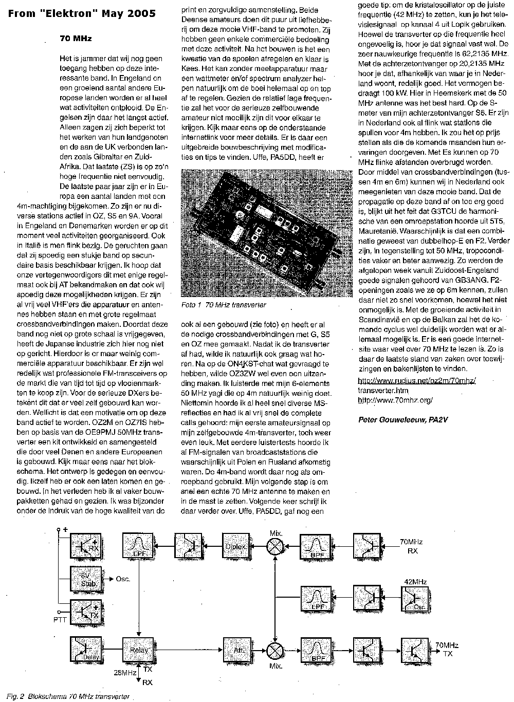
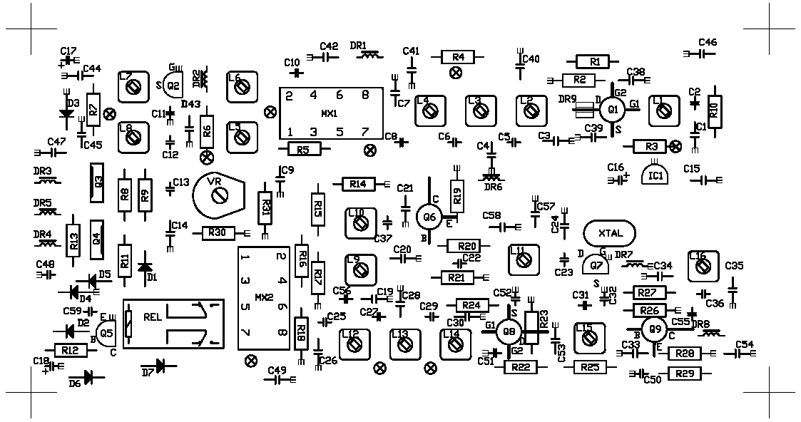
The 70 MHz input signal passes through the input filter (L1, C1, C2) to the input amplifier (BF988) where the gain is approx. 25 dB. Then through the band pass filter (L2 - 4, C3 - 8) providing a suitable selectivity.
The balanced mixer MX1 mixes the 70 MHz signal down to 28 MHz loosing approx. 6 dB in the process. Next the signal is amplified approx. 10 dB in a low noise J-FET (J310). The band-pass filter (L7/8 and C11 - 14) increases the selectivity considerably. Undesired products are decoupled via R5 in the L5/C9 diplexing filter.
For better stability the oscillator chain is supplied with 8 V from a 78L08 voltage regulator. The oscillator, another J310, oscillates on 42 MHz using a 3rd overtone crystal, series resonance. The 42 MHz signal is being amplified through Q6 to approx. 17 dBm/50 mW. In the following low-pass filter the harmonics are being attenuated. Then the signal is attenuated to approx. 7 dBm/5 mW through R14 - 18 which also provides impedance matching for the TX and RX mixers.
The transmit mixer, MX2, only needs approx. -15 dBm/30 µW 28 MHz IF signal from the transceiver. A suitable level can be achieved by adjusting VR in the attenuator (R30, R31 and VR). The resulting 70 MHz TX signal is then filtered through a three-stage band-pass filter (L12 - 14/C 25 - 30) before being amplified in a BF988, and finally a BFR96 to a level exceeding 100 mW. Through the final pi-filter (L16/C34 - C36) the TX signal reaches the output terminal.
The PTT circuit uses two BD442 for the RX/TX switching, TX when PTT is grounded. At the "DR4" terminal +12 V/1 A is available during TX. It is intended to switch the antenna relay and/or a PA. The circuit around the BC337 delays the TX key while activating the antenna relay immediately. This means that the TX output (70 OUT) is delayed approx. 100 ms after the antenna relay is activated. Consequently the antenna relay switches without any TX signal present.
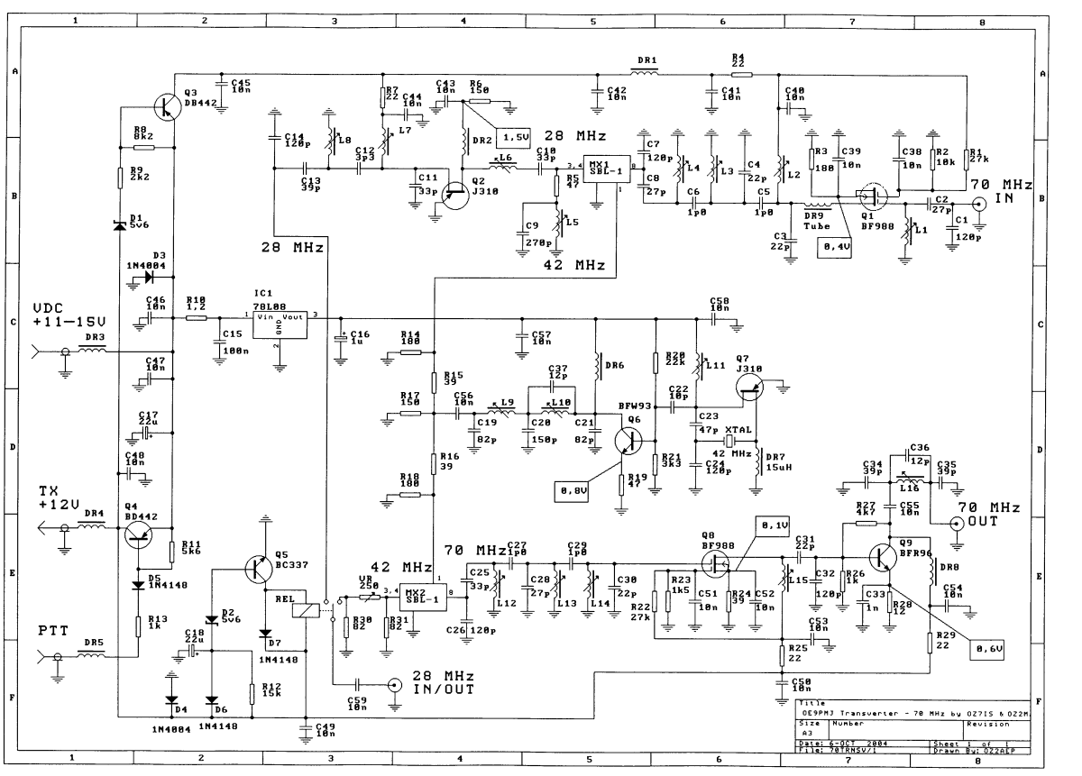
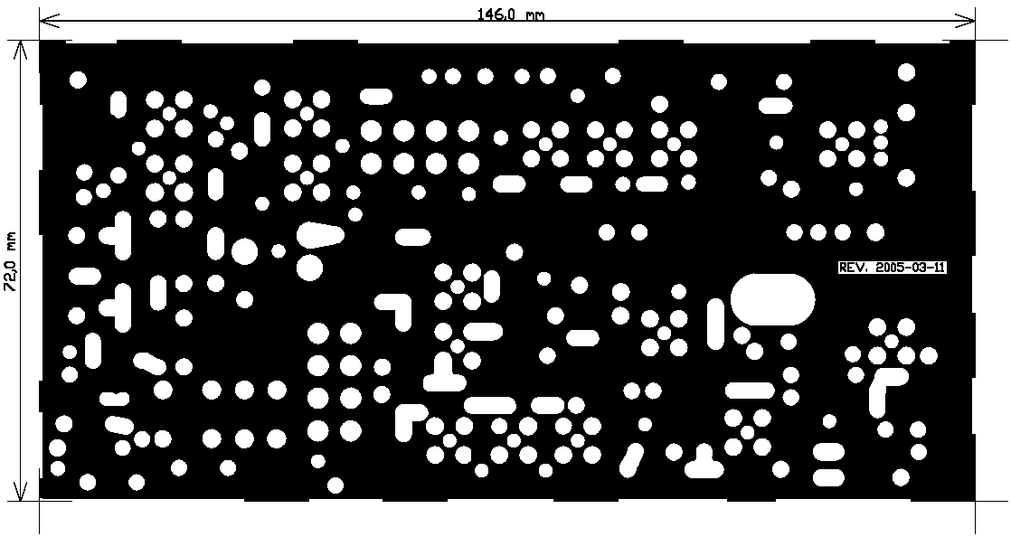
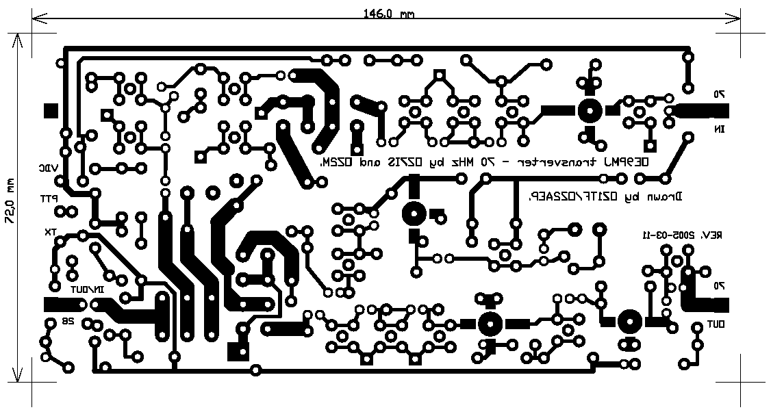
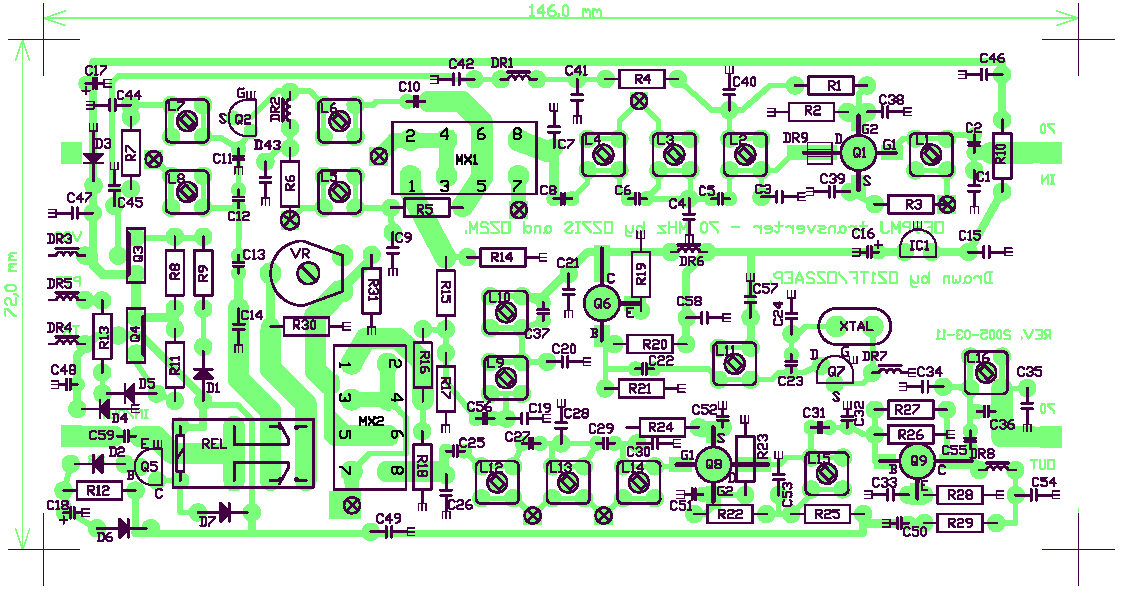
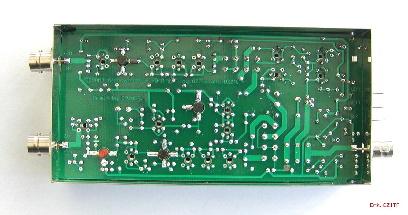
The complete transverter is build on a 1,5 mm double sided glass-fibre epoxy PCB to be fitted into a standard metal sheet box measuring 148 x 74 x 30 (50) mm3. The component (upper) side of the PCB is mainly a "ground plane". When drilling the PCB please remember to drill the "centre-hole" for the coils approx. 3,2 mm. Then it is possible to change the coil core without de-soldering the coil, in case of a broken core! The = indicates where the components are soldered directly onto the "ground-plane".
Initially all resistors and "vias" are mounted and soldered if not already embedded in the PCB. One end of R3 and 6 are soldered directly to the "ground-plane". Then the four "strip-line" transistors: 2 x BF988, BFW93 and BFR96 are soldered into place. Then follows the diodes, capacitors (short wires please!) and the rest of the components according to their heights. All components connected to ground are soldered to the upper side (ground-plane) of the PCB.
On the Neosid coils the "ground-flanges" of the copper housing needs to be cut before mounting, if mounted on a PCB without appropriate holes in it. When mounted, the copper housing of the coils are soldered directly to the "ground-plane" where indicated. If the coils have a fifth leg - NOT in a corner - it is cut off. On L6 to L11 and L16 it is clearly visible to which legs the coil is soldered to. Be sure to mount it correctly!
The RX/TX shift is done the way it is, due to the fact that some transceivers only have a single transverter RF connector, common for the RX input and the TX output. If you have separate connectors for RX and TX, the 28 MHz relay is not needed! Just attach a short piece of coax from the point of the incoming 28 MHz point of the (now missing) relay, to the unused pad close below D3.
Then mount the screen over the oscillator and fit the small screen on the bottom side. Finally the tested PCB is soldered into the box, AFTER drilling the holes for connectors, feed through capacitors, etc.!
If you have access to a range of suitable instruments you should wait mounting the mixers, Q2 and the relay. In this case it will be an advantage to sweep the front end with its filters (70 MHz), the diplexer (28 MHz), the IF amplifier (28 MHz), the low-pass filter in the oscillator (42 MHz) and the transmitter (70 MHz).
Please note the components locations on home made PCBs: (×) denotes a "via" from top to bottom layer. ≡ denotes that the component must be soldered to ground on the top layer. Square pads, on the bottom layer denotes that the component must be soldered on both sides.
If the TX-IF-signal source is not adjustable and the TX mixer is fed with the proper levels, it is possible to introduce an adjustable TX output by changing the gate 2 voltage on Q8 (BF988). This can be done fixed or adjustable by connecting gate 2 to an external potentiometer in stead of R23. Remember to make a de-coupling similar to the one on DR3 - DR5.
First of all the oscillator is started. If not oscillating from the start, turn the core of L11 until the voltage across R19 suddenly changes from approx. 0,1 V to 0,8 V. The core is left between the upper and lower position where it stops oscillating, i.e. 0,1 V across R19. Check whether the oscillator starts again after the voltage has been removed for a while - BEFORE you continue the adjustment procedure!
The coils L9 and L10 are adjusted for maximum 42 MHz RF signal on pin 1 of the mixers. At the same point the frequency is verified with a counter. As the 70 MHz band only covers 500 (700) kHz the simplest way possible is to adjust the transverter on a frequency near the centre of the band while making some simple measurements. The best way would be to sweep it, but the simpler method is acceptable.
With a suitable signal around 70,200 MHz, the coils L1 - 8 are adjusted for maximum reading on the S-meter of the 28 MHz receiver. Verify at the band edges as well.
Same principle is used when adjusting the transmitter chain. Inject a 28,2 MHz signal, connect the PTT terminal to grounded and with a RF milli-voltmeter adjusted L12 to L16 is for maximum reading at 70,2 MHz. Here too you can verify the readings at the band edges. The 28,2 MHz carrier, max. 1 mW, is adjusted on VR, counter clockwise, until the signal on MX2 pin 3 or 4 is approx. one third of the oscillator signal. In case of difficulties in measuring this, the 28 MHz drive signal is reduced to the point where the 70 MHz output first starts to drop.
Please do not use a metal screw driver when adjusting the coils. Use a plastic screw driver or even better a real trimmer with a brass blade.
Below are a handful of aligning hints from many of the builders who are already on the air. Basically what you need as a minimum is a 70 MHz signal source, plus/minus some kHz is fine, and a RF diode probe and a voltmeter. Do not let the number of instruments scare you from being QRV on 70 MHz with your own kit.
Alternatively you may contact one of the voluntary alignment supporters listed on the main 70 MHz kits page.
Receiver chain
As signal source you may use one of the following for aligning the RX:
Peak the RX chain for maximum signal. When done adjust L1 for best signal to noise ratio using a weak 70 MHz signal.
Transmitter chain
A dummy load is nice to have at hand but you can do without it.
For aligning the TX just peak all the TX-chain coils for max output on the RF diode probe/watt-meter or alternative receiver.
Reduce the drive so you never exceed 150 mW output from the transverter.
Oscillator
To adjust the oscillator, L11, adjust the voltage as described across R19. The final adjustment can be done on the band with a know signal source either from a beacon or nearby station.
You can also use one of the many spectrum analyser programs available. Set your RX to the desired frequency - 1 kHz and start the program. When the signal is exactly at the 1 kHz you are on the right frequency with the oscillator.
Adjust L9 and L10 for maximum 42 MHz using the RF diode probe or receiver. Alternatively tune for max 70 MHz output in TX mode.
After sweeping the filters mount the remaining components (mixers, Q2 and the relay). Connect a spectrum analyzer to pin 1 on one of the mixers. Adjust L10 until the 84 MHz, the second harmonic, is maximally attenuated. It may cost you up to 0,5 dB on the 42 MHz signal, but the 84 MHz will be approx. 75 dB below the level of the 42 MHz signal. If you do it "by ear" it may only be 50 dB below.
Then connect the spectrum analyzer to the 70 MHz TX output (70 OUT) and adjust L16 for max attenuation of the second harmonic on 140 MHz. It will affect the desired signal, but only with a few tenths of a dB! On the other hand, the second harmonic should be at least 60 dB below the desired 70 MHz signal.
| General |
Operational frequency span |
: : |
69,9 MHz - 70,6 MHz 27,9 MHz - 28,6 MHz |
| TX |
Output power |
: : : : |
>100 mW -15 dBm - 0 dBm/30 µW - 1 mW, adjustable* 25 dB - 40 dB >60 dB |
| RX |
Gain |
: : : : : : |
ca. 23 dB <2,5 dB 0 dBm/1 mW 7 dBm/5 mW 98 dB 94 dB |
*: An input level up to 5 W is possible if changing the TX IF attenuator accordingly. Power resistors for this purpose is not included in the kit.
Fig 1. RX front-end passband characteristics. TV channel 4 is attenuated by 12 dB and the FM-band beyond 68 dB.
![]()
Fig 2. TX third order intermodulation distortion at 22 dBm/159 mW PEP.
![]()
Fig 3. TX spurious at 21 dBm/125 mW. All spurious are more than -65 dBc.
![]()
If you have bought a kit please see the list of the delivered components and changes etc.
| Resistor | Value |
| R1, R22 | 27 kΩ |
| R2 | 10 kΩ |
| R3, R14, R18 | 180 Ω |
| R4, R7, R25, R29 | 22 Ω |
| R5, R19 | 47 Ω |
| R6, R17 | 150 Ω |
| R8 | 8,2 kΩ |
| R9 | 2,2 kΩ |
| R10 | 1,2 Ω |
| R11 | 5,6 kΩ |
| R12 | 15 kΩ |
| R13, R26 | 1 kΩ |
| R15, R16, R24 | 39 Ω |
| R20 | 22 kΩ |
| R21 | 3,3 kΩ |
| R23 | 1,5 kΩ |
| R27 | 4,7 kΩ |
| R28 | 12 Ω |
| R30, R31 | 82 Ω |
| VR | 250 Ω |
All resistors are 0,25 W/0,4 W and metalfilm type.
| Capacitor | Value |
| C1, C7, C14, C24, C26, C32 | 120 pF |
| C2, C8, C28 | 27 pF |
| C3, C4, C30, C31 | 22 pF |
| C5, C6, C27, C29 | 1 pF |
| C9 | 270 pF |
| C10, C11, C25 | 33 pF |
| C12 | 3,3 pF |
| C13, C34, C35 | 39 pF |
| C15 | 100 nF, polyester, 2-modules |
| C16 | 1 µF, 16 V, electrolytic, axial |
| C17, C18 | 22 µF, 16 V, electrolytic, axial |
| C19, C21 | 82 pF |
| C20 | 150 pF |
| C22 | 10 pF |
| C23 | 47 pF |
| C33 | 1 nF |
| C36, C37 | 12 pF |
| C38-C59 | 10 nF |
All capacitors are 1 module, 2,54 mm, ceramic types unless otherwise stated.
| Component | Description |
| D1, D2 | 5,6 V zener diode, 0,5 W |
| D3, D4 | 1N4004 or equivalent |
| D5, D6, D7 | 1N4148 or equivalent |
| IC1 | 78L08 |
| MX1, MX2 | SBL-1, IE500, IE800, HPF505, MS85, MS83D |
| Q1, Q8 | BF988, BF981, BF900, BF960 |
| Q2, Q7 | J310, U310 |
| Q3, Q4 | BD442, BD434, BD438, BD136, BD140 |
| Q5 | BC337 |
| Q6 | BFW93, BFW92 |
| Q9 | BFR96 |
| Inductor | Description |
| DR1, DR2, DR3, DR4, DR5, DR6, DR8 | VK200, ~10 µH RF choke |
| DR7 | 15 µH RF choke |
| L1, L2, L3, L4, L12, L13, L14, L15 | Neosid 00 5231 03 |
| L6, L7, L8 | Neosid 00 5048 00 |
| L9, L10, L11 | Neosid 00 5049 00 |
| L5, L16 | Neosid 00 5061 00 |
| Component | Description |
| Ferrite beads | Mount on Q1 and Q8 drain |
| Crystal | 42 MHz, third overtone HC49/U |
| Metal sheet box | 148 x 74 x 30 (or 50) mm3. Schubert Weissblechgehäuse type. |
| BNC sockets | Three or four x UG290/U or UG447/U. Four needed if separate 28 MHz RX |
| Feed through capacitors | Three x 1 nF, solderable |
| Metal sheets | Big on top side, small on bottom side |
| Relay | Omron G5V-2, 12 V |
The original 50 MHz design by OE9PMJ had two IF options: 28 or 144 MHz. A 144 MHz IF for the 70 MHz version would need an oscillator on 74 MHz! This is simply to close to 70 MHz to keep the oscillator signal out of the desired pass band and is outside the scope of this 70 MHz design. Thus 144 MHz IF is not an option!
When writing this article more than 20 transverters of the above design are on the air in Europe. Some of these are fully home made others are kits that have been sold and the profit was used for supporting the operation of OZ7IGY that is no longer an EDR supported beacon.
Transverter
Mixers
|
Relay
Inductors Semiconductors |
Bo, OZ2M, www.rudius.net/oz2m